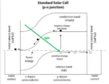
In a basic Schottky-junction (Schottky-barrier) solar cell, an interface between a metal and a semiconductor provides the band bending necessary for charge separation.[1] Traditional solar cells are composed of p-type and n-type semiconductor layers sandwiched together, forming the source of built-in voltage (a p-n junction).[2] Due to differing energy levels between the Fermi level of the metal and the conduction band of the semiconductor, an abrupt potential difference is created, instead of the smooth band transition observed across a p-n junction in a standard solar cell, and this is a Schottky height barrier.[3] Although vulnerable to higher rates of thermionic emission, manufacturing of Schottky barrier solar cells proves to be cost-effective and industrially scalable.[4]
However, research has shown thin insulating layers between metal and semiconductors improve solar cell performance, generating interest in metal-insulator-semiconductor Schottky junction solar cells. A thin insulating layer, such as silicon dioxide, can reduce rates of electron-hole pair recombination and dark current by allowing the possibility of minority carriers to tunnel through this layer.[5]
The Schottky-junction is an attempt to increase the efficiency of solar cells by introducing an impurity energy level in the band gap. This impurity can absorb more lower energy photons, which improves the power conversion efficiency of the cell.[6] This type of solar cell allows enhanced light trapping and faster carrier transport compared to more conventional photovoltaic cells.[7]
Material types
Schottky junction solar cells can be constructed using many different material types.
Cadmium selenide
One material is cadmium selenide.[8] As a direct bandgap semiconductor, CdSe has many applications in modern technology. Previous experiments using CdSe in solar cells resulted in a power-conversion efficiency of approximately 0.72%.[8] Liang Li et al. propose using single cadmium selenide nanobelts-on-electrodes. This method uses electron-beam lithography, or EBL, which provides a more efficient synthesis method to developing Schottky junction solar cells. Although this material does not provide a large power-conversion efficiency as of yet, the advent of simpler fabrication methods show promise in nano-electronic applications.[8] Further research is being conducted to increase the efficiency of cadmium selenide cells.
Nickel oxide
When constructing bulk-heterojunction solar cells, p-type nickel oxide is an effective anode layer. Its function as a wide band-gap semiconductor helps planarize the anode surface, and helps maximum photon flux to reach the active layer. In this case, NiO thickness was also measured, and increasing the thickness decreases cell efficiency. In these cells, nickel oxide replaces poly(3,4-ethylenedioxythiophene) polystyrene sulfonate, or PEDOT:PSS, resulting in a dramatic increases in performance while still maintaining stability of the cell. Compared to the cadmium selenide cell, nickel dioxide cells provide a power-conversion efficiency to 5.2%.[9]
Gallium arsenide
Under the right conditions, a gallium arsenide cell can produce an efficiency of around 22%. This is considered an MIS, or metal-insulator-semiconductor, and requires a thin oxide layer to prevent photo-current suppression.[10] Sheng S. Li et al. for the first time show that an effective barrier height equal to the band gap energy can be realized if the thickness and dopant density of the p-layer as well as the dopant density in the n substrate are properly chosen.[10]
References
- ↑ Tung, Raymond T. (2014). "The Physics and Chemistry of the Schottky Barrier Height". Applied Physics Reviews. 1 (1): 011304. Bibcode:2014ApPRv...1a1304T. doi:10.1063/1.4858400.
- ↑ Partain, Larry; Fraas, Lewis (2010). Solar Cells and Their Applications. Hoboken, New Jersey: John Wiley & Sons, Inc.
- ↑ Landsberg, P.T.; Klimpe, C. (1977). "Theory of the Schottky Barrier Cell" (PDF). Proceedings of the Royal Society of London. Series A, Mathematical and Physical Sciences. 354 (1676): 101–118. doi:10.1098/rspa.1977.0058. S2CID 97366390.
- ↑ Srivatava, S.; et al. (1980). "Efficiency of Schottky Barrier Solar Cells". Physica Status Solidi A. 58 (2): 343–348. Bibcode:1980PSSAR..58..343S. doi:10.1002/pssa.2210580203.
- ↑ Pulfrey, David L. (1978). "MIS Solar Cells: A Review". IEEE Transactions on Electron Devices. 25 (11): 1308–1317. Bibcode:1978ITED...25.1308P. doi:10.1109/t-ed.1978.19271. S2CID 47296128.
- ↑ Luque, Antonio; Martí, Antonio (1997). "Increasing the Efficiency of Ideal Solar Cells by Photon Induced Transitions at Intermediate Levels". Physical Review Letters. 78 (26): 5014–5017. Bibcode:1997PhRvL..78.5014L. doi:10.1103/physrevlett.78.5014.
- ↑ Fan, Guifeng; Zhu, Hongwei; Wang, Kunlin; Wei, Jinquan; Li, Xinming; Shu, Qinke; Guo, Ning; Wu, Dehai (2011). "Graphene/Silicon Nanowire Schottky Junction for Enhanced Light Harvesting". ACS Applied Materials & Interfaces. 3 (3): 721–725. doi:10.1021/am1010354. PMID 21323376.
- 1 2 3 Li, Liang; Lu, Hao; Deng, Kaimo (3 Dec 2012). "Single CdSe nanobelts-on-electrodes Schottky junction solar cells". Journal of Materials Chemistry A. 1 (6): 2089–2093. doi:10.1039/C2TA00410K.
- ↑ Irwin, Michael D.; Buchholz, Bruce; Hains, Alexander W.; Chang, Robert P. H.; Marks, Tobin J. (26 Feb 2008). "p-Type semiconducting nickel oxide as an efficiency-enhancing anode interfacial layer in polymer bulk-heterojunction solar cells". Proceedings of the National Academy of Sciences of the United States of America. 105 (8): 2783–2787. Bibcode:2008PNAS..105.2783I. doi:10.1073/pnas.0711990105. PMC 2268537.
- 1 2 Li, Sheng S. (Feb 1978). "Theoretical analysis of a novel MPN gallium arsenide Schottky barrier solar cell". Solid-State Electronics. 21 (2): 435–438. Bibcode:1978SSEle..21..435L. doi:10.1016/0038-1101(78)90274-5.
Further reading
- Memming, Rüdiger (2000). Semiconductor Electrochemistry (2 ed.). Wiley-VCH. pp. 26–38. doi:10.1002/9783527613069. ISBN 978-352731281-8. S2CID 30162712.