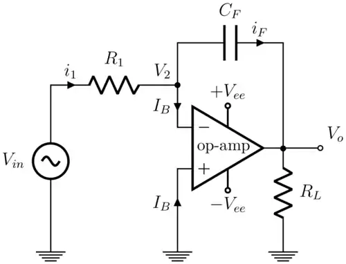
The operational amplifier integrator is an electronic integration circuit. Based on the operational amplifier (op-amp), it performs the mathematical operation of integration with respect to time; that is, its output voltage is proportional to the input voltage integrated over time.
Applications
The integrator circuit is mostly used in analog computers, analog-to-digital converters and wave-shaping circuits. A common wave-shaping use is as a charge amplifier and they are usually constructed using an operational amplifier though they can use high gain discrete transistor configurations.
Design
The input current is offset by a negative feedback current flowing in the capacitor, which is generated by an increase in output voltage of the amplifier. The output voltage is therefore dependent on the value of input current it has to offset and the inverse of the value of the feedback capacitor. The greater the capacitor value, the less output voltage has to be generated to produce a particular feedback current flow.
The input impedance of the circuit is almost zero because of the Miller effect. Hence all the stray capacitances (the cable capacitance, the amplifier input capacitance, etc.) are virtually grounded and they have no influence on the output signal.[1]
Ideal circuit
This circuit operates by passing a current that charges or discharges the capacitor during the time under consideration, which strives to retain the virtual ground condition at the input by off-setting the effect of the input current:

Referring to the above diagram, if the op-amp is assumed to be ideal, then the voltage at the inverting (-) input is held equal to the voltage at the non-inverting (+) input as a virtual ground. The input voltage passes a current through the resistor producing a compensating current flow through the series capacitor to maintain the virtual ground. This charges or discharges the capacitor over time. Because the resistor and capacitor are connected to a virtual ground, the input current does not vary with capacitor charge, so a linear integration that works across all frequencies is achieved (unlike RC circuit § Integrator).
The circuit can be analyzed by applying Kirchhoff's current law at the inverting input:
For an ideal op-amp, amps, so:
Furthermore, the capacitor has a voltage-current relationship governed by the equation:
Substituting the appropriate variables:
For an ideal op-amp, volts, so:
Integrating both sides with respect to time:
If the initial value of is assumed to be 0 volts, the output voltage will simply be proportional to the integral of the input voltage:[2]
Practical circuit
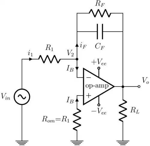
This practical integrator attempts to address a number of flaws of the ideal integrator circuit:

Real op-amps have a finite open-loop gain, an input offset voltage and input bias currents , which may not be well-matched and may be distinguished as going into the inverting input and going into the non-inverting input. This can cause several issues for the ideal design; most importantly, if , both the output offset voltage and the input bias current can cause current to pass through the capacitor, causing the output voltage to drift over time until the op-amp saturates. Similarly, if were a signal centered about zero volts (i.e. without a DC component), no drift would be expected in an ideal circuit, but may occur in a real circuit.
To negate the effect of the input bias current, it is necessary for the non-inverting terminal to include a resistor which simplifies to provided that is much smaller than the load resistance and the feedback resistance . Well-matched input bias currents then cause the same voltage drop of at both the inverting and non-inverting terminals, to effectively cancel out the effect of bias current at those inputs.
Also, in a DC steady state, an ideal capacitor acts as an open circuit. The DC gain of the ideal circuit is therefore infinite (or in practice, the open-loop gain of a non-ideal op-amp). To counter this, a large resistor may be inserted in parallel with the feedback capacitor. This limits the DC gain of the circuit to a finite value. Note that some op amps have a large internal feedback resistor, and many real capacitors have leakage that is effectively a large feedback resistor.[3]
The addition of these resistors turns the output drift into a finite, preferably small, DC error voltage:
Notes on offset: a variation of this circuit simply uses an adjustable voltage source instead of and some op amps with very low offset voltage may not even require offset correction.[4] Offset correction is a bigger concern for older op amps, particularly BJT types. Another variation circuit to avoid offset correction that works for AC signals only is to capacitively-couple the input with large input capacitor before which will naturally charge up to the offset voltage. Additionally, because offset may drift over time and temperature, some op amps provide null offset pins, which can be connected to a potentiometer whose wiper connects to the negative supply to allow readjusting when conditions change. These methods may be combined for greater ensurance.[3]
Frequency response
The ideal integrator's Bode plot has a steady -20 dB per decade over all frequencies. This negative slope corresponds to the time-domain integration property of the Laplace transform whose transfer function is simply (i.e. a pole at zero frequency).
The practical integrator is an active first-order low-pass filter with a gain relatively constant up to its pole (the -3 dB cutoff frequency) which is inversely proportional to the time constant:
Its gain then starts to decrease by 20 dB per decade, and for ideal op amps continues so indefinitely. However, real op amps have a limited gain-bandwidth product (GBWP). Integration only occurs over the -20 dB per decade slope, which is steady only from frequencies about a decade above to about a decade below the op amp's GBWP.[4]
For both circuits, the unity gain frequency is inversely proportional to the time constant:
References
- ↑ Transducers with Charge Output
- ↑ "AN1177 Op Amp Precision Design: DC Errors" (PDF). Microchip. 2 January 2008. Archived (PDF) from the original on 2019-07-09. Retrieved 26 December 2012.
- 1 2 Pavlic, Theodore (2009) [2007]. "Practical Integrators and Operational Amplifier Offset - Practical Integrators and Operational Amplifier Offset - ECE 327: Electronic Devices and Circuits Laboratory I" (PDF). Archived (PDF) from the original on 2022-10-11. Retrieved 2023-08-20.
- 1 2 "Analog Engineer's Circuit: Amplifiers - SBOA275A" (PDF). Texas Instruments. 2019 [2018]. Archived (PDF) from the original on 2022-09-01. Retrieved 2023-08-20.