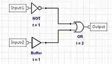
Glitch removal is the elimination of glitches—unnecessary signal transitions without functionality—from electronic circuits. Power dissipation of a gate occurs in two ways: static power dissipation and dynamic power dissipation. Glitch power comes under dynamic dissipation in the circuit and is directly proportional to switching activity. Glitch power dissipation is 20%–70% of total power dissipation and hence glitching should be eliminated for low power design.
Switching activity occurs due to signal transitions which are of two types: functional transition and a glitch. Switching power dissipation is directly proportional to the switching activity (α), load capacitance (C), Supply voltage (V), and clock frequency (f) as:
- P = α·C·V2·f
Switching activity means transition to different levels. Glitches are dependent on signal transitions and more glitches results in higher power dissipation. As per above equation switching power dissipation can be controlled by controlling switching activity (α), voltage scaling etc.
Glitch reduction techniques
Reducing switching activity
As discussed, more transition results in more glitches and hence more power dissipation. To minimize glitch occurrence, switching activity should be minimized. For example, Gray code could be used in counters instead of binary code, since every increment in Gray code only flips one bit.
Gate freezing
Gate freezing minimizes power dissipation by eliminating glitching. It relies on the availability of modified standard library cells such as the so-called F-Gate. This method consists of transforming high glitch gates into modified devices which filter out the glitches when a control signal is applied. When the control signal is high, the F-Gate operates as normal but when the control signal is low, the gate output is disconnected from the ground. As a result, it can never be discharged to logic 0 and glitches are prevented.
Hazard filtering and balanced path delay

Hazards in digital circuits are unnecessary transitions due to varying path delays in the circuit. Balanced path delay techniques can be used for resolving differing path delays. To make path delays equal, buffer insertion is done on the faster paths. Balanced path delay will avoid glitches in the output.
Hazard filtering is another way to remove glitching. In hazard filtering gate propagation delays are adjusted. This results in balancing all path delays at the output.
Hazard filtering is preferred over path balancing as path balancing consumes more power due to the insertion of additional buffers.
Gate sizing
Gate upsizing and gate downsizing techniques are used for path balancing. A gate is replaced by a logically equivalent but differently-sized cell so that delay of the gate is changed. Because increasing the gate size also increases power dissipation, gate-upsizing is only used when power saved by glitch removal is more than the power dissipation due to the increase in size. Gate sizing affects glitching transitions but does not affect the functional transition.
Multiple threshold transistor
The delay of a gate is a function of its threshold voltage. Non-critical paths are selected and threshold voltage of the gates in these paths is increased. This results in balanced propagation delay along different paths converging at the receiving gate. Performance is maintained since it is determined by the time required by the critical path. A higher threshold voltage also reduces the leakage current of a path.
See also
References
Further reading
- Hyungoo, Lee; Hakgun, Shin; Juho, Kim (2004). "Glitch Elimination by Gate Freezing, Gate Sizing and Buffer Insertion for Low Power Optimization Circuit". 30th Annual Conference of IEEE Industrial Electronics Society, 2004. IECON 2004. Vol. 3. pp. 2126–2131. doi:10.1109/IECON.2004.1432125. ISBN 978-0-7803-8730-0. S2CID 21217122.
- Coudert, Olivier (September 1997). "Gate Sizing for Constrained Delay/Power/Area Optimization" (PDF). IEEE Transactions on Very Large Scale Integration (VLSI) Systems. 5 (4): 465–472. CiteSeerX 10.1.1.474.766. doi:10.1109/92.645073.
- Sapatnekar, Sachin S.; Chuang, Weitong, Power-Delay Optimizations in Gate Sizing (PDF)
- Shum, Warren; Anderson, Jason H. (2011), FPGA Glitch Power Analysis and Reduction, International Symposium on Low power electronics and design (ISLPED), pp. 27–32
- Zhanping, Chen; Liqiong, Wei; Kaushik, Roy (March 1997), Reducing Glitching and Leakage Power in Low Voltage CMOS Circuits, Purdue University School of Electrical and Computer Engineering
External links
- Patent US6356101 B1: Glitch Removal Circuitary, 2002-03-12, http://www.google.co.in/patents/US6356101.
- https://learn.digilentinc.com/Documents/277